Quick facts
- Completely free and Open Source (including firmware)
- Programs PIC10-12-16-18-24, dsPIC30-33, ATMEL AVR (serial and HV serial programming), serial memories like 24xxxx (I2C), 25xxx (SPI), 93xx6 (MicroWire), DS24xx (OneWire), 11xxx (UNIO), communicates with generic I2C & SPI devices (see supported devices)
- Can work as ICD debugger with some PIC16F devices
- USB 2.0 Full Speed interface, HID class (same as keyboards, mice, etc.)
- Self powered
- Doesn't need drivers
- Built from easy to find components (estimated cost ~5€)
- Hardware generated timings for maximum speed and reliability (writes a 18F2550 in 10s)
- Doesn't saturate your CPU and doesn't suffer when other programs are running
- Open source control programs for Linux and Windows
- It's not another PicKit clone
Another programmer?
In the last few years [...so it was in 2007], as serial and parallel interfaces have almost disappeared, electronics enthusiasts find even more difficult to program microcontrollers; old time programmers don't work any more; common solutions include using USB to serial adapters (which can't accept direct access but only slow API calls), or add-on interface chips, like FTDIxxxx, which appear substantially as serial interfaces and require custom or proprietary drivers.So why not use PIC controllers and their native USB interface?
After searching a while I couldn't find an USB programmer which was at the same time functional, free, and open source, so I decided to design one.
Open source means that all sources and schematics are given free of charge with the rights to modify and release them.
USB & HID firmware (v0.12.0)
In order to use the USB interface included in some PIC devices we need a firmware that implements one of the classes defined by the USB consortium or a new one; I opted for the HID class, which is supported natively by all operating systems and so doesn't need any driver. Maximum allowed speed is 64KB/s, although with my application I measured something in the range 20-40 KB/s, certainly enough to program devices with memory of 100KB at most.Like all USB devices this one too has a vid and a pid; these are usually obtained under payment; I got a combination for free from pid.codes: 0x1209&0x5432; anyways it's possible to configure both, so I leave the choice to the user.
The programmer appears to the system as a HID device that exchanges 64 bytes packets every 1 ms.
The USB firmware comes from a nearly unknown open source project, written by Alexander Enzmann, which I modified and adapted to the MCC18 compiler.
I wrote a brief guide on how to use it; to my knowledge this is the only open source firmware with HID support and GPL license.
My programmer code simply adds a command interpreter that drives the microcontroller's outputs according to a set of instructions.
The main control cycle waits for a packet from USB, then executes commands in sequence while managing communication tasks; at the same time a control function is called periodically by a timer interrupt and keeps the DCDC regulator output voltage constant.
Building the project requires only free programs: MPLAB and MCC18 student version, which are unfortunately only available for the windows (in)operating system.
It's certainly possible to compile with SDCC, but some changes are needed to the source code.
Everything is given under the GPL2 license.
Here is the complete MPLABX project;
here the compiled hex file for 18F2550;
here the version for 18F25K50.
Control programs
I initially thought of modifying an existing software, for example winpic or picprog, but I found it would be too difficult because I use packetized communications instead of serial; so I had to write one (two) from scratch.Unfortunately, or fortunately, since I'm not a professional software developer I kept features at minimum; the result are very small but fast programs that don't use your CPU for nothing.
For most devices the code is verified while programming; for the others immediately following the writing phase.
Ideally you should have the same version number for both software and firmware, except for the last number which indicates minor changes and bug fixes; however I tried to keep the same protocol with each release, so that apart from new features it is often possible to use new software with older firmware and vice versa.
In case you wonder, the reason why it's not possible to program directly from MPLAB is not technical: Microchip does not release specifications of how to interface with its program; if you want them you have to be a commercial manufacturer and sign a non disclosure agreement, which is clearly impossible for a GPL2 open source project.
On the contrary, integration with Piklab is possible and I hope will be done soon; right now the custom programmer interface lacks some essential parameters, but whoever has the ability and time can fix it for sure.
GTK graphical interface for Windows and Linux (v0.12.2)
OPGUI uses the GTK2 libraries so under Windows it's necessary to install the GTK Runtime Environment(64 bit).A screenshot of Opgui:
A quick guide: buttons to read, write, load and save files are on the toolbar.
The "Data" tab shows what the programmer is doing.
On the "Device" tab it's possible to choose the device and modify some programming options, such as writing ID and calibration words, using the eeprom etc.; only settings compatible with the current device are considered.
Under "Options" are various general settings: USB connection, errors, log file, expansion boards; using the "Hardware Test" function and a voltmeter is possible to check that the circuit is working.
The "I2C/SPI" tab is useful for communicating with generic I2C and SPI devices; in case of I2C it's always necessary to specify the control byte (and address, if not zero); RW bit is handled automatically.
For example, to write manually 3 bytes on a 24xx16 at address 64 write: A0 40 1 2 3
From version 0.7.10 it includes an ICD debugger for (some) 16F devices, working more or less like pdb; in addition it supports coff files.
The "I/O" tab allows to control individual I/O lines and the power supplies.
Under "Utility" there are functions to convert a single hex line to data and vice versa.
There is no installer since there aren't any libraries and the executable is very small.
The program accepts hex8 and hex32 files, and also binary files in case of serial memories.
Supported languages are currently English and Italian; to add other languages it's necessary to generate the languages.rc file (-langfile option) and to modify it; the language id is before the respective strings, enclosed in square brackets [].
The language is chosen at startup by matching the system language (it can also be forced with -lang).
In order to give access to the hardware under Linux see Accessing hardware under Linux.
You can find more info on the OpenProg and Opgui user's guide or in the source code guide.
To compile the program from source (optional) you need to install the GTK libraries, GCC and the maketools (MinGW/MSYS in Windows); then write:
> make
To install it under Linux(if you wish):
> make install
Download the compiled program ... or the sources.
Command-line utility (Linux and Windows, v0.12.0)
OP is a command-line executable; the Windows version doesn't need installation;If not otherwise specified, it looks for an USB device with vid&pid=0x1209:0x100.
It supports hex8 and hex32 files, and also binary files in case of serial memories.
Using the --HWtest option and a voltmeter is possible to check that the circuit is working.
It is possible to communicate with generic I2C/SPI devices; in case of SPI it's always necessary to specify control byte and address (or addresses); the RW bit is handled automatically.
In case of problems or just for curiosity it's possible to log all data exchanged with the programmer with option -l; its optional parameter must be specified with -l=<file> (who knows why? It may be a bug of getopt).
Supported languages are currently English and Italian; more languages can be added by generating and modifying the file languages.rc.
Options:
-BKosccal load BKosccal from file
-calib load calibration from file
-command <message> send <message> to the programmer and exit
-cwX <cw> force config word X
-d, device <dev.> device
-ee use eeprom
-err <max> max errors during writing
-fuse <val> write fuse low byte (Atmel only)
-fuseh <val> write fuse high byte (Atmel only)
-fusex <val> write extended fuse byte (Atmel only)
-h, help help
-HWtest hardware test
-i, info informations about programmer
-i2c_r <N Ctr Addr> read N bytes from I2C bus
-i2c_r2 <N Ctr Addr(2)> read N bytes from I2C bus (16b address)
-i2c_w <N Ctr Addr Data> write N bytes to I2C bus
-i2c_w2 <N Ctr Addr(2) Data> write N bytes to I2C bus (16b address)
-i2cspeed <speed> set I2C speed: 0=100k, 1=200k, 2=400k, 3=800k
-icd <val> enable ICD (goto address)
-id use ID
-l, log [=file] save log
-lang <language> load <language> strings
-langfile write all strings to file
-lock <val> write lock byte (Atmel only)
-mode <mode> SPI mode: 00,01,10,11
-osccal loads osccal from file instead of using the value saved before erase
-p, path <path> programmer path [/dev/usb/hidrawX]
-pid <pid> programmer pid [0x5432]
-r, reserved read reserved area
-rep <n> report size [64]
-s1, S1 Multiple programming triggered by S1
-s, save <file> save Ihex file
-se, saveEE <file> save EEPROM on Ihex file (ATxxxx only)
-spi_r <N> read N bytes from SPI bus
-spi_w <N Data> write N bytes to SPI bus
-spispeed <speed> set SPI speed: 0=100k,1=200k,2=300k,3=500k
-support supported devices
-use_BKosccal copy BKosccal to osccal
-v, version version
-vid <vid> programmer vid [0x1209]
-w, write <file> write Ihex file
-we, writeEE <file> write EEPROM on Ihex file (ATxxxx only)
Examples:
> op -h #help
> op -d 18F2550 -ee -s read.hex #reads code and EEPROM and saves to file
> op -d 16F628 -ee -w write.hex #writes
> op -i2c_r 8 A0 0 #reads 8 bytes from I2C bus, control byte A0, address 0
A frequent error is to write the device name with lowercase letters instead of uppercase:
write 16F628, not 16f628
In order to give access to the hardware under Linux see Accessing hardware under Linux.
A makefile is included, so to build the application you need GCC and the maketools (MinGW/MSYS on Windows); write:
> make
Then to install it (if you wish):
> make install
You can find more info in the source code guide.
Also included is Hid_test, an utility to send and receive a single 64 bit packet; it can be useful for experimenting with the hardware; in theory one could even write a complete programming script using it.
Download
Accessing hardware under Linux
Under Linux the apps look for device /dev/hidrawX (/dev/usb/hiddevX before 0.11.2) and need read/write rights on it; it is also possible to specify the device path manually.To give the rights to all users you can type:
>sudo chmod a+r /dev/hidraw1
To permanently enable a user do the following (on Ubuntu and other Debian based distributions, check for others):
as root create a file /etc/udev/rules.d/10-openprogrammer.rules
if you want to enable a user group write:
KERNEL=="hidraw[0-9]", ATTRS{idProduct}=="5432", ATTRS{idVendor}=="1209", GROUP="<group>", SYMLINK+="openprogrammer"
where <group> is one of the user groups (to get a list type "groups"); select a suitable group and if your user desn't belong to it execute "addgroup <user> <group>"
or, if you want to enable all users, change reading permissions:
KERNEL=="hidraw[0-9]", ATTRS{idProduct}=="5432", ATTRS{idVendor}=="1209", MODE="0664", SYMLINK+="openprogrammer"
restart udev to apply changes:
> udevadm control --reload-rules
> udevadm trigger
Now, every time the system detects the programmer, the corresponding /dev/hidrawX has the correct permissions and also the link /dev/openprogrammer is created.
If after plugging the programmer you can't find /dev/hidrawX (and LED2 doesn't blink at 1 Hz), it's sufficient to execute a few times lsusb to force enumeration, or unplug and replug the cable.
MFC Graphical interface (not updated any more: v0.9.1)
OpenProg is a C++ application written with Visual C++ 6 and MFC.Only the basic programming functions are implemented; it was the fist GUI of the project, but currently development continues only on OP/OPGUI.
It has the advantage of working without any additional library.
Download application ... or sources (Visual Studio 6 workspace)
How to ...
Erase a device: every device is erased before being programmed; however if you still need to erase it it's sufficient to write a hex file with valid data (i.e. <0xFF) beyond the implemented memory.For example, here how it would look for PIC12-16:
:020000040000FA
:0144010000BA
:00000001FF
And for PIC18:
:020000040002F8
:020000000000FE
:00000001FF
Another method: OPGUI starts up with all memory buffers filled with 0xFF; just write on any device without loading first, it will erase it and quit.
Change Configuration Word: Config words are usually specified in the hex file, but can be forced for PIC 10-12-16-18 using the related device options (or via command line).
It's also possible to recompile sources, otherwise to change the hex file directly; in case of most PIC16 the config word is at address 0x2007, which is stored at 0x400E; the last byte of the line is a checksum, which can be calculated as the two's complement of the sum of all bytes in the line.
For example:
:02400E00xxxxCC , where xxxx is the new value and CC the checksum
Change configuration of Atmel AVR: unlike PICs, these devices do not map their configuration words in the main memory area (so the hex files don't specify any configuration) and it's necessary to write the desired Fuse/Lock bytes in the device options; don't write anything in case the default value is fine for the application.
Solve the "Synchronization error" with AVR devices: A possible cause is that the SPI speed is too high in relation to the CPU speed; the latter has to be > 4 x SPI speed.
There are many possible CPU speed configurations, so the (new) algorithm varies the SPI speed automatically in order to enter Program Mode.
Obviously the lower the speed the longer it takes to read/write the device; in order to speed up operations you could write an empty file with a fast CPU configuration, then write the final file and configuration at high speed.
Some devices include an extremely low speed setting (16 kHz), which is too low even for the adaptive algorithm; in this case use "write Fuse Low @ 3 kHz" to change Fuse Low to a higher speed setting, then write in the usual way.
Another cause could be that the serial programming is disabled: this can be done only using a parallel programmer, and the same is necessary to enable it again.
The third possibility is that the device is configured for external resonator but X2 cannot move; in case you use the AVR expansion board make sure X2 is not tied to GND.
Check that a device is blank: read it and look at displayed data; only lines with valid data are displayed, so if there are none the device is blank.
Verify that a write was successful: all write algorithms implement write verification, either during write or immediately after; if the program reports 0 errors it means that the code was succesfully verified.
If you want to check again you can read the device and compare with the original data; keep in mind that frequently not all bits are implemented; for example in PIC16 a data word is 14 bits long, so even if the source data is 0xFFFF it will be written as 0x3FFF; also the Config Words usually have some bits fixed at 0, which are not checked.
Read the reserved memory area: most PIC devices have a reserved area above the Config Words which is used for test or calibration purposes; to see it use the relative option before read; on PIC24-30-33 the executive memory is read as well.
Correctly use OscCal and other calibration words: some devices (eg. 12F5xx) store the internal oscillator calibration value in the last address of program memory and in a backup location past the ID words; after erasing all memory the control programs restore the calibration value taking it from the backup location, unless specified otherwise; other options are: use the old value (which should be the same as the backup, if none was changed before), use what is specified in the .hex file.
Similarly it's possible to overwrite the backup value with the content of the .hex file, using option "write ID and BKosccal"; in this case the ID locations will be written as well, if specified in the .hex file.
To overwrite the other calibration values use option "write Calib1 and 2".
Supported devices
I tried this programmer with a small number of devices (those I own plus some tested by other users) indicated in bold; the other devices are supported but not tested; however, considering that for every device family at least one has been verified, all of them should work without problems.Please let me know if you verify operation with the untested devices.
Also contact me if you need other algorithms or code new ones by yourself.
Take notice:
LF series PICs are used exactly as the F ones;
Atmel AVR devices with varius suffixes are grouped together whenever the programming algorithm is exactly the same, eg. ATmega8 and ATmega8A;
EEPROM memories comprise all versions with VDDmax=5V, eg. 242LC56, 24AA256, etc.;
93x memories use 2 different algorithms, for the 93S series and for all the others, indicated with 93x (93xA have 8 bit organization);
SPI Flash memories need a low voltage adapter (see the schematic diagrams).
Devices supported for read and write:
10F200, 10F202, 10F204, 10F206, 10F220, 10F222, 10F320, 10F322,
12C508, 12C508A,12C509, 12C509A, 12F508, 12F509, 12F510, 12F519,
12F609, 12F615, 12F617, 12F629, 12F635, 12F675, 12F683,
12F752, 12F529T39, 12F529T48,
12F1501, 12F1571, 12F1572, 12F1612, 12F1822, 12F1840,
16F505, 16F506, 16F526, 16F527, 16F54, 16F57, 16F570, 16F59,
16F610, 16F616, 16F627, 16F627A, 16F628, 16F628A, 16F630, 16F631, 16F636, 16F639, 16F648A, 16F676, 16F677, 16F684, 16F685, 16F687, 16F688, 16F689, 16F690,
16F707, 16F716, 16F72, 16F720, 16F721, 16F722, 16F722A, 16F723, 16F723A, 16F724, 16F726, 16F727, 16F73, 16F737, 16F74, 16F747, 16F753, 16F76, 16F767, 16F77, 16F777, 16F785,
16F818, 16F819, 16C83, 16F83, 16F83A, 16C84, 16F84, 16F84A, 16F87, 16F870, 16F871, 16F872, 16F873, 16F873A, 16F874, 16F874A, 16F876, 16F876A, 16F877, 16F877A, 16F88, 16F882, 16F883, 16F884, 16F886, 16F887,
16F913, 16F914, 16F916, 16F917, 16F946,
16F1454, 16F1455, 16F1459, 16F1503, 16F1507, 16F1508, 16F1509, 16F1512, 16F1513, 16F1516, 16F1517, 16F1518, 16F1519, 16F1526, 16F1527, 16LF1554, 16LF1559, 16F1574, 16F1575, 16F1578, 16F1579, 16F1613, 16F1614, 16F1615, 16F1618, 16F1619, 16F1703, 16F1704, 16F1705, 16F1707, 16F1708, 16F1709, 16F1713, 16F1716, 16F1717, 16F1718, 16F1719, 16F1764, 16F1765, 16F1768, 16F1769, 16F1773, 16F1776, 16F1777, 16F1778, 16F1779, 16F1782, 16F1783, 16F1784, 16F1786, 16F1787, 16F1788, 16F1789, 16F1823, 16F1824, 16F1825, 16F1826, 16F1827, 16F1828, 16F1829, 16F1847, 16LF1902, 16LF1903, 16LF1904, 16LF1906, 16LF1907, 16F1933, 16F1934, 16F1936, 16F1937, 16F1938, 16F1939, 16F1946, 16F1947,
16F15213, 16F15214, 16F15223, 16F15224, 16F15225, 16F15243, 16F15244, 16F15245, 16F15254, 16F15255, 16F15256, 16F15274, 16F15275, 16F15276, 16F15313, 16F15323, 16F15324, 16F15325, 16F15344, 16F15345, 16F15354, 16F15355, 16F15356, 16F15375, 16F15376, 16F15385, 16F15386,
16F17114, 16F17115, 16F17124, 16F17125, 16F17126, 16F17144, 16F17145, 16F17146, 16F17154, 16F17155, 16F17156, 16F17174, 16F17175, 16F17176,
16F18013, 16F18014, 16F18015, 16F18023, 16F18024, 16F18025, 16F18026, 16F18044, 16F18045, 16F18046, 16F18054, 16F18055, 16F18056, 16F18074, 16F18075, 16F18076,
16F18114, 16F18115, 16F18124, 16F18125, 16F18126, 16F18144, 16F18145, 16F18146, 16F18154, 16F18155, 16F18156, 16F18174, 16F18175, 16F18176,
16F18313, 16F18323, 16F18324, 16F18325, 16F18326, 16F18344, 16F18345, 16F18346, 16F18424, 16F18425, 16F18426, 16F18444, 16F18445, 16F18446, 16F18455, 16F18456, 16F18854, 16F18855, 16F18856, 16F18857, 16F18875, 16F18876, 16F18877,
16F19155, 16F19156, 16F19175, 16F19176, 16F19185, 16F19186, 16F19195, 16F19196, 16F19197,
18F04Q40, 18F04Q41, 18F05Q40, 18F05Q41, 18F06Q40, 18F06Q41, 18F14Q40, 18F14Q41, 18F15Q40, 18F15Q41, 18F16Q40, 18F16Q41,
18F242, 18F248, 18F252, 18F258, 18F442, 18F448, 18F452, 18F458, 18F1220, 18F1230, 18F1320, 18F1330, 18F13K22, 18F13K50, 18F14K22, 18F14K50, 18F2220, 18F2221, 18F2320, 18F23K20, 18F23K22, 18F2321, 18F2331, 18F2410, 18F24J10, 18F24J11, 18F2420, 18F24K20, 18F24K22, 18F2423, 18F2431, 18F2439, 18F2450, 18F24J50, 18F24K50, 18F2455, 18F2458, 18F24Q71, 18F2480, 18F2510, 18F25J10, 18F25J11, 18F2515, 18F2520, 18F25K20, 18F25K22, 18F2523, 18F2525, 18F2539, 18F25K42, 18F25Q43, 18F2550, 18F25J50, 18F25K50, 18F2553, 18F25Q71, 18F2580, 18F25K80, 18F25K83, 18F2585, 18F2610, 18F26J11, 18F26J13, 18F2620, 18F26K20, 18F26K22, 18F26K42, 18F26Q43, 18F26J50, 18F26K50, 18F26J53, 18F26Q71, 18F2680, 18F26K80, 18F2682, 18F26K83, 18F26Q83, 18F26Q84, 18F2685, 18F27J13, 18F27K42,, 18F27Q43 18F27J53, 18F27Q83, 18F27Q84, 18F4220, 18F4221, 18F4320, 18F43K20, 18F43K22, 18F4321, 18F4331, 18F4410, 18F44J10, 18F44J11, 18F4420, 18F44K20, 18F44K22, 18F4423, 18F4431, 18F4439, 18F4450, 18F44J50, 18F4455, 18F4458, 18F44Q71, 18F4480, 18F4510, 18F45J10, 18F45J11, 18F4515, 18F4520, 18F45K20, 18F45K22, 18F4523, 18F4525, 18F4539, 18F45K42, 18F45Q43, 18F4550, 18F45J50, 18F45K50, 18F4553, 18F45Q71, 18F4580, 18F45K80, 18F4585, 18F4610, 18F46J11, 18F46J13, 18F4620, 18F46K20, 18F46K22, 18F46K42, 18F46Q43, 18F46J50, 18F46K50, 18F46J53, 18F46Q71, 18F4680, 18F46K80, 18F4682, 18F46Q83, 18F46Q84, 18F4685, 18F47J13, 18F47K42, 18F47Q43, 18F47J53, 18F47Q83, 18F47Q84, 18F54Q71, 18F55K42, 18F55Q43, 18F55Q71, 18F56K42, 18F56Q43, 18F56Q71, 18F56Q83, 18F56Q84, 18F57K42, 18F57Q43, 18F57Q83, 18F57Q84,
18F63J11, 18F63J90, 18F64J11, 18F64J90, 18F65J10, 18F65J11, 18F65J15, 18F65J50, 18F65J90, 18F65K80, 18F66J10, 18F66J11, 18F66J15, 18F66J16, 18F66J50, 18F66J55, 18F66J60, 18F66J65, 18F66J90, 18F66J93, 18F67J10, 18F67J11, 18F67J50, 18F67J60, 18F66K80, 18F67J90, 18F67J93, 18F83J11, 18F83J90, 18F84J11, 18F84J90, 18F85J10, 18F85J11, 18F85J15, 18F85J50, 18F85J90, 18F8520, 18F86J10, 18F86J11, 18F86J15, 18F86J16, 18F86J50, 18F86J55, 18F86J60, 18F86J65, 18F86J72, 18F86J90, 18F86J93, 18F8722, 18F87J10, 18F87J11, 18F87J50, 18F87J60, 18F87J72, 18F87J90, 18F87J93, 18F96J60, 18F96J65, 18F97J60,
24F04KA200, 24F04KA201, 24F08KA101, 24F08KA102, 24F16KA101, 24F16KA102, 24FJ16GA002, 24FJ16GA004, 24FJ32GA002, 24FJ32GA004, 24FJ32GA102, 24FJ32GA104, 24FJ32GB002, 24FJ32GB004, 24FJ48GA002, 24FJ48GA004, 24FJ64GA002, 24FJ64GA004, 24FJ64GA006, 24FJ64GA008, 24FJ64GA010, 24FJ64GA102, 24FJ64GA104, 24FJ64GA306, 24FJ64GA308, 24FJ64GA310, 24FJ64GB002, 24FJ64GB004, 24FJ64GB106, 24FJ64GB108, 24FJ64GB110, 24FJ64GC006, 24FJ64GC008, 24FJ64GC010, 24FJ96GA006, 24FJ96GA008, 24FJ96GA010, 24FJ128GA006, 24FJ128GA008, 24FJ128GA010, 24FJ128GA106, 24FJ128GA108, 24FJ128GA110, 24FJ128GA306, 24FJ128GA308, 24FJ128GA310, 24FJ128GB106, 24FJ128GB108, 24FJ128GB110, 24FJ128GB206, 24FJ128GB210, 24FJ128GC006, 24FJ128GC008, 24FJ128GC010, 24FJ128DA106, 24FJ128DA110, 24FJ128DA206, 24FJ128DA210, 24FJ192GA106, 24FJ192GA108, 24FJ192GA110, 24FJ192GB106, 24FJ192GB108, 24FJ192GB110, 24FJ256GA106, 24FJ256GA108, 24FJ256GA110, 24FJ256GB106, 24FJ256GB108, 24FJ256GB110, 24FJ256GB206, 24FJ256GB210, 24FJ256DA106, 24FJ256DA110, 24FJ256DA206, 24FJ256DA210,
24EP32GP202, 24EP32GP203, 24EP32GP204, 24EP32MC202, 24EP32MC203, 24EP32MC204, 24EP64GP202, 24EP64GP203, 24EP64GP204, 24EP64GP206, 24EP64MC202, 24EP64MC203, 24EP64MC204, 24EP64MC206, 24EP128GP202, 24EP128GP204, 24EP128GP206, 24EP128MC202, 24EP128MC204, 24EP128MC206, 24EP256GP202, 24EP256GP204, 24EP256GP206, 24EP256MC202, 24EP256MC204, 24EP256MC206, 24EP512GP202, 24EP512GP204, 24EP512GP206, 24EP512MC202, 24EP512MC204, 24EP512MC206,
24HJ12GP201, 24HJ12GP202, 24HJ16GP304, 24HJ32GP202, 24HJ32GP204, 24HJ32GP302, 24HJ32GP304, 24HJ64GP202, 24HJ64GP204, 24HJ64GP206, 24HJ64GP210, 24HJ64GP502, 24HJ64GP504, 24HJ64GP506, 24HJ64GP510, 24HJ128GP202, 24HJ128GP204, 24HJ128GP206, 24HJ128GP210, 24HJ128GP306, 24HJ128GP310, 24HJ128GP502, 24HJ128GP504, 24HJ128GP506, 24HJ128GP510, 24HJ256GP206, 24HJ256GP210, 24HJ256GP610,
30F1010, 30F2010, 30F2011, 30F2012, 30F2020, 30F2023, 30F3010, 30F3011, 30F3012, 30F3013, 30F3014, 30F4011, 30F4012, 30F4013, 30F5011, 30F5013, 30F5015, 30F5016, 30F6010, 30F6011, 30F6012, 30F6013, 30F6014, 30F6015,
33FJ06GS101, 33FJ06GS102, 33FJ06GS202, 33FJ12GP201, 33FJ12GP202, 33FJ12MC201, 33FJ12MC202, 33FJ16GP304, 33FJ16GS402, 33FJ16GS404, 33FJ16GS502, 33FJ16GS504, 33FJ16MC304, 33FJ32GP202, 33FJ32GP204, 33FJ32GP302, 33FJ32GP304, 33FJ32GS406, 33FJ32GS606, 33FJ32GS608, 33FJ32GS610, 33FJ32MC202, 33FJ32MC204, 33FJ32MC302, 33FJ32MC304, 33FJ64GP202, 33FJ64GP204, 33FJ64GP206, 33FJ64GP306, 33FJ64GP310, 33FJ64GP706, 33FJ64GP708, 33FJ64GP710, 33FJ64GP802, 33FJ64GP804, 33FJ64GS406, 33FJ64GS606, 33FJ64GS608, 33FJ64GS610, 33FJ64MC202, 33FJ64MC204, 33FJ64MC506, 33FJ64MC508, 33FJ64MC510, 33FJ64MC706, 33FJ64MC710, 33FJ64MC802, 33FJ64MC804, 33FJ128GP202, 33FJ128GP204, 33FJ128GP206, 33FJ128GP306, 33FJ128GP310, 33FJ128GP706, 33FJ128GP708, 33FJ128GP710, 33FJ128GP802, 33FJ128GP804, 33FJ128MC202, 33FJ128MC204, 33FJ128MC506, 33FJ128MC510, 33FJ128MC706, 33FJ128MC708, 33FJ128MC710, 33FJ128MC802, 33FJ128MC804, 33FJ256GP506, 33FJ256GP510, 33FJ256GP710, 33FJ256MC510, 33FJ256MC710,
33EP32GP502, 33EP32GP503, 33EP32GP504, 33EP32MC202, 33EP32MC203, 33EP32MC204, 33EP32MC502, 33EP32MC503, 33EP32MC504, 33EP64GP502, 33EP64GP503, 33EP64GP504, 33EP64GP506, 33EP64MC202, 33EP64MC203, 33EP64MC204, 33EP64MC206, 33EP64MC502, 33EP64MC503, 33EP64MC504, 33EP64MC506, 33EP128GP502, 33EP128GP504, 33EP128GP506, 33EP128MC202, 33EP128MC204, 33EP128MC206, 33EP128MC502, 33EP128MC504, 33EP128MC506, 33EP256GP502, 33EP256GP504, 33EP256GP506, 33EP256MC202, 33EP256MC204, 33EP256MC206, 33EP256MC502, 33EP256MC504, 33EP256MC506, 33EP512GP502, 33EP512GP504, 33EP512GP506, 33EP512MC202, 33EP512MC204, 33EP512MC206, 33EP512MC502, 33EP512MC504, 33EP512MC506,
AT90S1200, AT90S2313, AT90S8515, AT90S8535, ATmega48, ATmega8, ATmega88, ATmega8515, ATmega8535, ATmega16, ATmega164, ATmega168, ATmega32, ATmega324, ATmega328, ATmega64, ATmega644, ATmega1284,
ATtiny11, ATtiny12, ATtiny13, ATtiny2313, ATtiny24, ATtiny25, ATtiny26, ATtiny261, ATtiny4313, ATtiny44, ATtiny45, ATtiny461, ATtiny48, ATtiny84, ATtiny85, ATtiny88, ATtiny861,
2400, 2401, 2402, 2404, 2408, 2416, 2432, 2464, 24128, 24256, 24512, 241024, 241025,
25010, 25020, 25040, 25080, 25160, 25320, 25640, 25128, 25256, 25512, 251024,
95010, 95020, 95040, 95080, 95160, 95320, 95640, 95128, 95256, 95512, 95M01, 95M02,
251005, 252005, 254005, 258005, 251605, 25X05, 25X10, 25X20, 25X40, 25X80, 25X16, 25X32, 25X64, 25X128, 25Q40,
93S46, 93x46, 93x46A, 93S56, 93x56, 93x56A, 93S66, 93x66, 93x66A, 93x76, 93x76A, 93x86, 93x86A,
DS2430, DS2431, DS2433, DS28EC20, DS1820,
11010, 11020, 11040, 11080, 11160
devices supported for read only:
12C671, 12C672, 12CE673, 12CE674
Important!! Don't use 3.3V devices without the 3.3V expansion boards, otherwise permanent damage may occur; the software verifies that such adapters are present before starting to program, but obviously you need to select the proper device; the 3.3V devices are:
12F1xxx,16F1xxx,18FxxJxx,18FxxKxx,24Fxxx,24Hxxx,33Fxxx.
Some of them have 5V variants; if you need to program at 5V you can select the option "Don't require LV boards". Also don't put any 24F-33F on the 30F socket, which works at 5V.
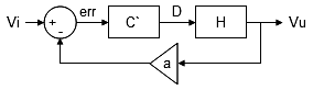
Communication protocol
To design a communication protocol we must take into account some often contrasting requirements:transfer speed and efficiency, code size, adaptability and expandability.
Differently from serial links, USB is packet based; a packet is received altogether, but HID devices can only exchange them every ms, so it is out of question to manage timings directly as with serial ports.
It's necessary to introduce synthetic commands that the microcontroller can use to recreate the proper waveforms.
Furthermore, one objective of a reliable programmer is to be independent from the host speed and CPU occupation, so the task of generating waveforms would anyways be given to the microcontroller.
In general we can find two types of programmers: simple serial programmers only take commands to change voltage levels; host software manages both timings and programming algorithms but needs all the CPU time and is dramatically affected by other processes running on the system.
At the other extreme are "smart" programmers, which autonomously manage timings and algorithms, but must be updated to support new devices and tend to require much memory to store code.
I chose a combination of both: ICSP (In Circuit Serial Programming) commands are implemented in firmware, but the host software manages the algorithms.
In order to increase speed and efficiency some instructions correspond to sequences of frequently repeated commands, such as sequential reads.
The advantage of this approach is that timings are very precise, while the extreme variety of algorithms does not increase the firmware code size.
Another advantage is that once the basic commands are verified the development of algorithms is done on the PC, without the need for frequent firmware updates.
For example, this is the sequence used to enter program mode for 16F628 and read DevID:
SET_PARAMETER //set delays to be used by other instructions
SET_T1T2 //T1 & T2
1 //T1=1us
100 //T2=100us
EN_VPP_VCC //Vpp & Vcc = 0
0x0
SET_CK_D //Clock and Data as output and 0
0x0
EN_VPP_VCC //Vpp enabled
0x4
NOP //small delay
EN_VPP_VCC //Vdd+Vpp enabled
0x5
NOP //small delay
LOAD_CONF //program counter to 0x2000
0xFF //fake config
0xFF //fake config
INC_ADDR_N //increment address by 6
0x06
READ_DATA_PROG //read DevID
...
In addition to ICSP commands other instructions manage the programmer, control programming voltages, execute precise delays, communicate via I2C or SPI bus.
Every instruction is executed in at least 40 us, due to the interpreter loop execution time.
ICSP commands use T1 or T2 as values for delays; all instructions return an echo, with the exception of FLUSH, which immediately sends the output buffer and stops the execution of current packet.
In case an instruction doesn't have enough parameters it returns an error (0xFE) and the execution of current packet is halted.
The state of USB connection is signaled by LED2: it blinks at 4 Hz during enumeration, at 1 Hz in normal operation.
LED1 shows when there are instructions being executed.
Following is the list of all instructions:
| Instruction | Value | Parameters | Answer | Notes |
| NOP | 0x00 | none | echo | no operation |
| PROG_RST | 0x01 | none | echo + 10B | programmer reset; sends fw version (3B), ID (3B), " RST" string |
| PROG_ID | 0x02 | none | echo+ 6B | sends fw version (3B), ID (3B) |
| CHECK_INS | 0x03 | 1B | echo + 1B | if specified instruction exists returns its code, otherwise returns error (0xFE) |
| FLUSH | 0x04 | none | none | flushes output buffer (sends 64B) and stops command interpreter for the current packet. |
| VREG_EN | 0x05 | none | echo | turns on the voltage regulator |
| VREG_DIS | 0x06 | none | echo | turns off the voltage regulator |
| SET_PARAMETER | 0x07 | 1B | echo | sets internal parameters; byte1: parameter to change, byte 2-3 value: SET_T1T2 (=0): T1 & T2 SET_T3 (=1): T3(H,L) SET_timeout (=2): timeout(H,L) SET_MN (=3): M, N |
| WAIT_T1 | 0x08 | none | echo | waits T1 us (1us default) |
| WAIT_T2 | 0x09 | none | echo | waits T2 us (100us default) |
| WAIT_T3 | 0x0A | none | echo | waits T3 us (2ms default) |
| WAIT_US | 0x0B | 1B | echo | waits N us |
| READ_ADC | 0x0C | none | echo +2B | reads regulator voltage (effective 10bits, MSB-LSB); considering the input divider, voltage in V is <value>/1024*5*34/12 |
| SET_VPP | 0x0D | 1B | echo +1B | sets regulator voltage to <parameter>/10; if error is < 200 mV within 15ms returns <parameter>, otherwise error (0xFE) |
| EN_VPP_VCC | 0x0E | 1B | echo | controls Vpp and Vcc on the programmed device; 1 bit for level (0-1), 1bit for impedance (keep at 0); bit 0-1: Vcc, bit 2-3: Vpp |
| SET_CK_D | 0x0F | 1B | echo | controls CK, D, PGM on the programmed device; 1 bit for level (0-1), 1bit for impedance (low-high); bit 0-1: D, bit 2-3: CK, bit 4-5: PGM |
| READ_PINS | 0x10 | none | echo +1B | reads the state of control lines, 1 bit level (0-1), 1bit impedence (low-high); bit 0-1: D, bit 2-3: CK, bit 4-5: PGM |
| LOAD_CONF | 0x11 | 2B | echo | ICSP command: Load configuration (000000), T1 us between command and data; 14 bit data (right aligned, MSB-LSB) |
| LOAD_DATA_PROG | 0x12 | 2B | echo | ICSP command: Load Data in Program Memory (000010), T1 us between command and data; 14 bit data (right aligned, MSB-LSB) |
| LOAD_DATA_DATA | 0x13 | 1B | echo | ICSP command: Load Data in Data Memory (000011), T1 us between command and data; 8 bit data |
| READ_DATA_PROG | 0x14 | none | echo +2B | ICSP command: Read Data from Program Memory (000100), T1 us between command and data; 14 bit data (right aligned, MSB-LSB) |
| READ_DATA_DATA | 0x15 | none | echo +1B | ICSP command: Read Data from Data Memory (000101), T1 us between command and data; 8 bit data |
| INC_ADDR | 0x16 | none | echo | ICSP command: Increment Address (000110), T1 us delay at the end |
| INC_ADDR_N | 0x17 | 1B | echo | ICSP command: Increment Address (000110), T1 us delay at the end; repeated N times |
| BEGIN_PROG | 0x18 | none | echo | ICSP command: Begin Programming (001000) |
| BULK_ERASE_PROG | 0x19 | none | echo | ICSP command: Bulk Erase Program Memory (001001) |
| END_PROG | 0x1A | none | echo | ICSP command: End Programming (001010) |
| BULK_ERASE_DATA | 0x1B | none | echo | ICSP command: Bulk Erase Data Memory (001011) |
| END_PROG2 | 0x1C | none | echo | ICSP command: End Programming (001110) |
| ROW_ERASE_PROG | 0x1D | none | echo | ICSP command: Row Erase Program Memory (010001) |
| BEGIN_PROG2 | 0x1E | none | echo | ICSP command: Begin Programming (0011000) |
| CUST_CMD | 0x1F | 1B | echo | ICSP command specified in the parameter |
| PROG_C | 0x20 | 2B | echo +1B | Programs a word following 12Cxxx algorithm: 000010, 001000, 001110, M pulses & N overpulses |
| CORE_INS | 0x21 | 2B | echo | PIC18 ICSP command: Core instruction (0000); 16 bit data (MSB-LSB) |
| SHIFT_TABLAT | 0x22 | none | echo +1B | PIC18 ICSP command: Shift TABLAT (0010); 8 bit data |
| TABLE_READ | 0x23 | none | echo +1B | PIC18 ICSP command: Table read (1000); 8 bit data |
| TBLR_INC_N | 0x24 | 1B | echo+N+NB | PIC18 ICSP command: Table read post-inc (1001); 8 bit data; repeats N times; returns N and NB data |
| TABLE_WRITE | 0x25 | 2B | echo | PIC18 ICSP command: Table write (1100); 16 bit data (MSB-LSB) |
| TBLW_INC_N | 0x26 | (2N+1)B | echo | PIC18 ICSP command: Table write post-inc (1101); 16 bit data (MSB-LSB); repeats N times (N is the first parameter) |
| TBLW_PROG | 0x27 | 4B | echo | PIC18 ICSP command: Table write and program (1111); 16 bit data (MSB-LSB); also executes a NOP with a delay specified in parameters 3-4 (in us) |
| TBLW_PROG_INC | 0x28 | 4B | echo | PIC18 ICSP command: Table write and program post-inc (1110); 16 bit data (MSB-LSB); also executes a NOP with a delay specified in parameters 3-4 (in us) |
| SEND_DATA | 0x29 | 3B | echo | PIC18 ICSP command specified in byte 1; sends 16 bit data (MSB-LSB) |
| READ_DATA | 0x2A | 1B | echo+1B | PIC18 ICSP command specified in byte 1; reads 8 bit data |
| I2C_INIT | 0x2B | 1B | echo | Initializes I2C communication: 0xFF disables I2C; bit 6: slew rate control for speed > 100kbps; bit 5:3 speed: 0=100k, 1=200k, 2=400k, 3=800k, 4=1M; attention: use pull-up resistors according to selected speed; bit 2:0: logic level of A2-A1-A0 (on device) |
| I2C_READ | 0x2C | 3B | echo+1+NB | Reads <parameter 1> bytes from I2C bus using <parameter 2> as control byte and <parameter 3> as address; forces automatically the RW bit in the control byte. Responds with <parameter 1> + Data or with ACK_ERR (0xFD) in case of acknowledge error (eg. if there are no devices on the bus) |
| I2C_WRITE | 0x2D | 3B+NB | echo | Writes <parameter 1> bytes to I2C bus using <parameter 2> as
control byte and <parameter 3> as address; forces
automatically the RW bit in the control byte. Responds
with ACK_ERR (0xFD) in case of acknowledge error (eg. if there are
no devices on the bus). For 2 byte addresses just use the 2nd byte of address as the first byte of data. |
| I2C_READ2 | 0x2E | 4B | echo+1+NB | Reads from I2C bus; identical to I2C_READ, but uses 2 bytes for addressing |
| SPI_INIT | 0x2F | 1B | echo | Initializes SPI communication: 0xFF disables SPI bit 1:0 speed: 0=100kbps, 1=200kbps, 2=300kbps, 3=500kbps bit 2:3 SPI mode |
| SPI_READ | 0x30 | 1B | echo+1+NB | Reads <parameter 1> bytes from SPI bus. Returns <parameter 1> + Data; If <parameter 1>=0 returns the byte that was last received (during either read or write) |
| SPI_WRITE | 0x31 | 1B+NB | echo+1B | Writes <parameter 1> bytes to SPI bus. |
| EXT_PORT | 0x32 | 2B | echo | Forces levels of communication ports: <parameter 1> = <RB7:RB0> <parameter 2> = <RC7,RC6,RA5:RA3> Does not change signal direction. |
| AT_READ_DATA | 0x33 | 3B | echo+1+2NB | ATMEL command: read program memory (0010H000); reads <parameter 1> words at address <parameter 2> : <parameter 3> via SPI. Returns <parametro 1> + Data |
| AT_LOAD_DATA | 0x34 | 3B+2N | echo+1B | ATMEL command: load program memory page (0100H000); loads <parameter 1> words at address <parameter 2> : <parameter 3> via SPI. Returns <parameter 1> |
| CLOCK_GEN | 0x35 | 1B | echo | Generates a clock signal on RB3 (using CCP1-2 and TIMER1) bit 2:0 frequency: 0=100kHz, 1=200kHz, 2=500kHz, 3=1MHz, 4=2MHz, 5=3MHz, 6=6MHz; Disables PWM1 output (DCDC regulator) |
| SIX | 0x36 | 3B | echo | PIC24 ICSP command: Core instruction (0000); 24 bit data (MSB first) |
| REGOUT | 0x37 | none | echo +2B | PIC24 ICSP command: Shift out VISI register (0001); 16 bit data |
| ICSP_NOP | 0x38 | none | echo | PIC24 ICSP command: Execute NOP (0000) |
| TX16 | 0x39 | 1+2NB | echo+1B | Transmits 16 bit words over ICSP (MSB first); clock period: 2*(T1-1)+1 us |
| RX16 | 0x3A | 1B | echo+1+2NB | Receives 16 bit words over ICSP (MSB first); clock period: 2*(T1-1)+1 us |
| uW_INIT | 0x3B | none | echo | Initializes MicroWire communication |
| uW_TX | 0x3C | 1B+NB | echo+1B | Writes <parameter 1> bits to MicroWire bus. Data is specified MSB first |
| uW_RX | 0x3D | 1B | echo+1+NB | Reads <parameter 1> bits from MicroWire bus. Returns <parameter 1> + Data, MSB first |
| SIX_LONG | 0x3E | 3B | echo | PIC24 ICSP command: Core instruction (0000); 24 bit data (MSB first); appends 2 ICSP_NOP at the end |
| SIX_N | 0x3F | 1+3NB | echo | PIC24 ICSP command: Core instruction (0000); N * 24 bit data (MSB first); sends N instructions and adds M ICSP_NOP after each one; N=<parameter1>&0x3F, M=<parameter1> >>6 |
| OW_RESET | 0x40 | no | echo+1B | OneWire Reset pulse; detects the slave presence pulse: 1=present 0=absent |
| OW_WRITE | 0x41 | 1B+NB | echo | Writes <parameter 1> bytes on the OneWire bus |
| OW_READ | 0x42 | 1B | echo+1+NB | Reads <parameter 1> bytes from the OneWire bus |
| UNIO_STBY | 0x43 | no | echo | UNIO standby pulse |
| UNIO_COM | 0x44 | 1B+1B+NB | echo+1+NB | Executes a UNIO communication cycle: writes <parameter 1> bytes and reads <parameter 2> bytes; generates a synchronization byte if there are bytes to write |
| SET_PORT_DIR | 0x45 | 2B | echo | Sets the direction on the IO ports (0=out, 1=in): <parameter 1> = <RB7:RB0> <parameter 2> = <RC7,RC6,RA5:RA3> |
| READ_B | 0x46 | no | echo+1B | Reads IO port B |
| READ_AC | 0x47 | no | echo+1B | Reads IO ports A and C: <RC7,RC6,RA5:RA3> |
| AT_HV_RTX | 0x48 | 1B+2NB | echo+1B | Sends 2N*8 bits on RB0/RC7 (PB1/PB0), with CLK on RC6 (PB3) byte N=PB1, byte N+1=PB0 Receives 8 bits from RB1 (PB2) (only the last byte) |
| SIX_LONG5 | 0x49 | 3B | echo | PIC24 ICSP command: Core instruction (0000); 24 bit data (MSB first); appends 5 ICSP_NOP at the end |
| LOAD_PC | 0x50 | 2B | echo | ICSP command: Load PC address (011101), T1 us between command and data; 16 bit data (right aligned, MSB-LSB) |
| LOAD_DATA_INC | 0x51 | 2B | echo | ICSP command: Load data in NVM memory and increase address (100010), T1 us between command and data; 14 bit data (right aligned, MSB-LSB) |
| READ_DATA_INC | 0x52 | no | echo+2B | ICSP command: Read data from NVM memory and increase address (100100), T1 us between command and data; 14 bit data (right aligned, MSB-LSB) |
| JTAG_SET_MODE | 0x53 | 1B | echo | JTAG SET MODE: 6 bit data |
| JTAG_SEND_CMD | 0x54 | 1B | echo | JTAG COMMAND: 5 bit data |
| JTAG_XFER_DATA | 0x55 | 4B | echo+4B | JTAG TRANSFER DATA: 32 bit data MSB-LSB |
| JTAG_XFER_F_DATA | 0x56 | 4B | echo+4B | JTAG TRANSFER FAST DATA: 32 bit data MSB-LSB |
| ICSP8_SHORT | 0x57 | 1B | echo | 8-bit ICSP command without data: command code in <parameter1> |
| ICSP8_READ | 0x58 | 1B | echo+2B | 8-bit ICSP command with 16 bit data read: command code in <parameter1> |
| ICSP8_LOAD | 0x59 | 3B | echo | 8-bit ICSP command with 16 bit data write: command code in <parameter1> |
| READ_RAM | 0xF0 | 2B | echo+3B | Reads from host memory; 16 bit address, 8 bit data; echoes address |
| WRITE_RAM | 0xF1 | 3B | echo+3B | Writes to host memory; 16 bit address, 8 bit data; echoes address and data |
| LOOP | 0xF2 | none | none | Resets instruction pointer and executes all instructions again. For test purposes only. |
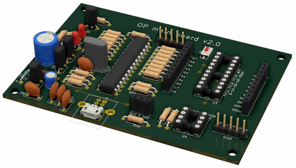
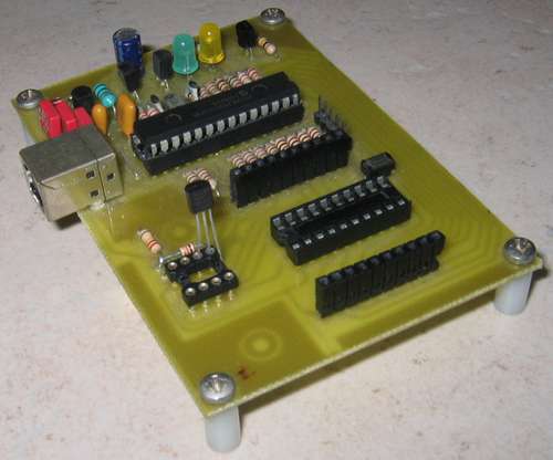
The circuit (v2.1)
The functionality of this programmer depends from two sections: the USB communication interface and the voltage generation circuit.In order to implement an USB pheripheral with a PIC micro we need very few components besides the the main microcontroller: a quartz, some capacitors, and a USB type B (or micro-B) receptacle, exactly as described in Microchip's application notes.
The voltage generation section requires some digital IO lines, some selectable power supplies, and a high voltage source; VCC and VPP are controlled using three transistors; VPP comes from a DCDC step-up converter formed by Q4, L1, D3 which is described later.
The main microcontroller is a 28 pin 18F2550 or a 18F25K50; the latter does not even need the quartz nor C2-C3.
Another advantage of the 18F25K50 is that it can be programmed with a low voltage programmer, like one built out of an Arduino or ESP8266 etc.
Yet another possible model is the 18F2553, which differs by its 12 bit ADC, so it requires firmware recompilation.
Using the corresponding 40 pin devices (4550, 45K50, 4553) requires modification of the circuit, keeping the same port assignments; the additional resources, however, will stay unused.
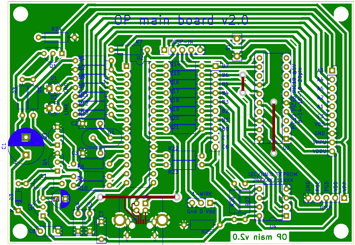
The schematic diagram was drawn using KiCad; below the main board:

Many components are optional, are only needed to program some types of devices or for future applications: connectors CONN2-3-4-5-6, protection resistors R11:23, I2C pull-up resistors R26-27, S1 switch, unused target sockets.
Component list:
- U1 12Mhz quartz (not necessary when using the 25K50; also 4, 8, 16, 20 MHz: reconfiguration of input divider options is required)
- U2 18F2550 or 18F25K50 (also 2553, 4550, 45K50, 4553, see above)
- U3 20pin socket.
- U4 8pin socket.
- Q1-Q2 BC557 (or any PNP, pay attention to polarity)
- Q3-Q4 BC547 (or any NPN, pay attention to polarity)
- D1-D2 LED
- D3 1N4148 (or any diode, better if Shottky)
- L1 100µH (resistor type or other)
- R1 22KΩ
- R2 12KΩ
- R3 100KΩ
- R4:6 10KΩ
- R7 1MΩ
- R8-R9 2.2KΩ
- R10 3.3KΩ
- R11:23 100Ω
- R24-R25 330KΩ
- R26-R27 10KΩ
- C1 22-100µF 25V
- C2-C3 22pF
- C4 >= 220nF
- C5 100nF
- C6 10µF
- C7-C8 100nF
- CONN1 USB type B or CONN1B1 type micro-B
- CONN2-3 10 pin female stripline
- CONN4-5 5 pin stripline
- CONN6 3 pin female stripline
A working circuit blinks D2 at 4Hz until the enumeration is completed, then at 1Hz.
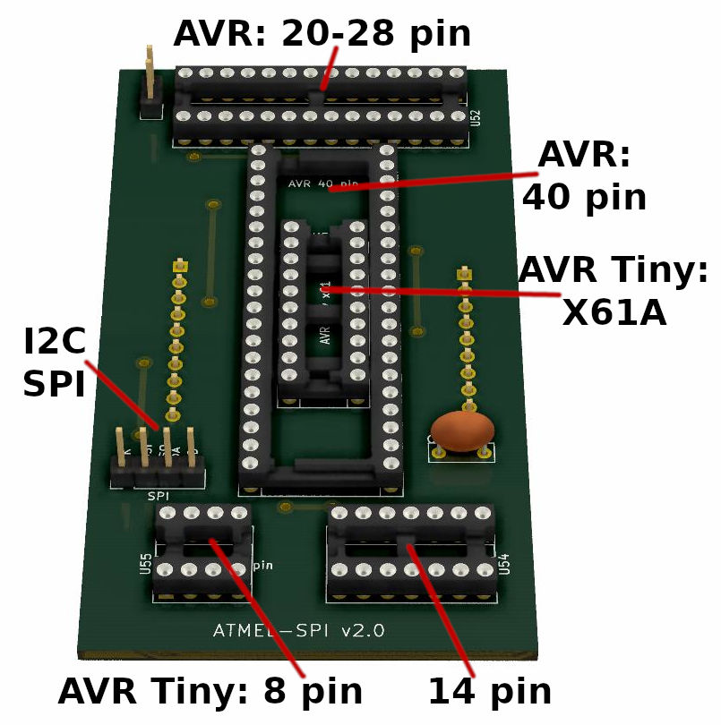
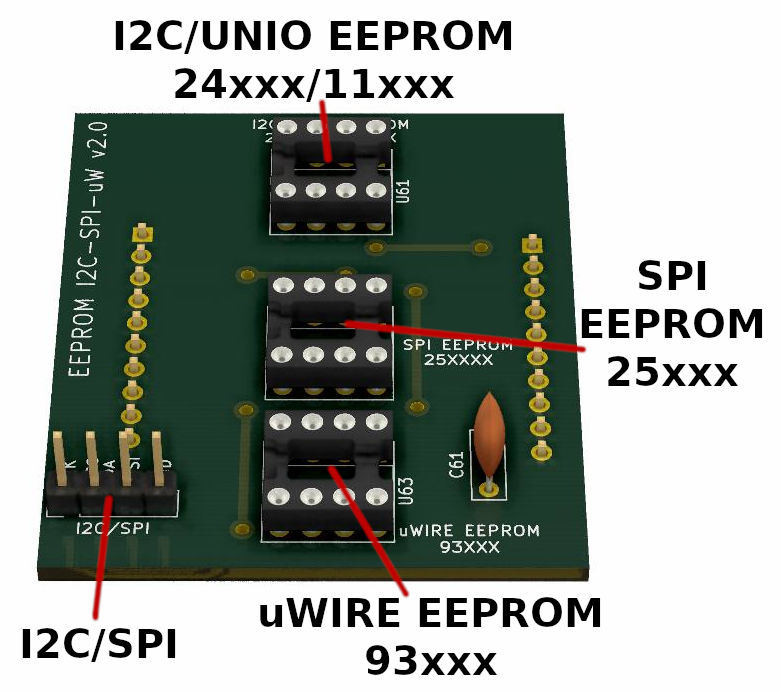
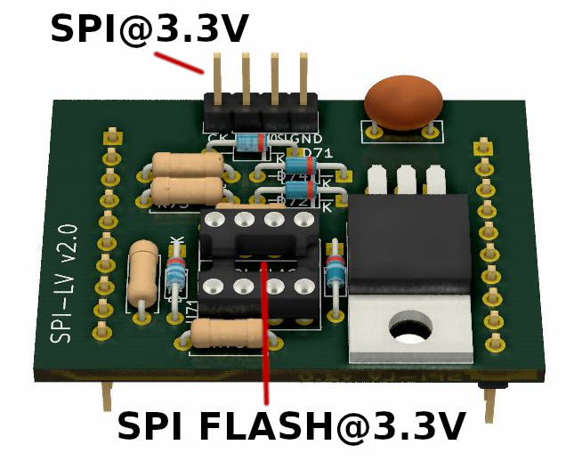
Additional devices can be programmed using expansion boards plugged to connectors CONN2-3:
- 28-40 pin PIC
- 8-20 pin PIC (same as main board, but there's more space for a ZIF socket)
- 3.3V PIC16-18 (this board includes a 3.3V regulator)
- PIC24-30-33 (this board includes a 3.3V regulator)
- I2C, SPI, microWire memories
- 3.3V SPI memories (this board includes a 3.3V regulator)
- 8-14-20-28-40 pin ATMEL AVR
In assembling the adapters I suggest to insert the expansion connectors from the component side, and keep their plastic spacer on that side; this improves the solder strength, especially during extraction.
To verify that everything is working correctly use the "Hardware Test" function in the control program: in this mode, to be executed without target devices, various combinations of outputs (CK, D, PGM, VDDU, VPPU, available on pins 14-15-12-1-4 of U3) are activated in sequence; if the measured voltages (with respect to GND, pin 5) correspond to what is presented on screen then the hardware is correctly assembled.
VPP voltage could be different from the set value by up to 1V; this is due to the fact that the DCDC converter takes VCC as reference voltage; the latter comes from the USB cable and can vary from 4.75V to 5.25V; in addition the feedback voltage divider (R1-R2) can introduce another 5% of error.
The most common causes of malfunction are:
incorrect orientation of transistors,
incorrect inductor value,
pcb defects like shorts or opens,
unsoldered capacitors,
main microcontrollorer not programmed or incorrectly programmed (often with wrong config words, e.g. with LVP option set).
Here you find the complete kicad project.
This is the old version drawn with gEDA.
PCB
The PCB was optimized to be produced at home, so it mostly uses the solder side; however a few jumpers are needed on the component side (a double side PCB would of course not need any). Traces are quite wide except in a few critical points.In case you choose the SMD micro-USB connector it is advisable to use a double-side PCB.
If you order the PCB from a commercial manufacturer you can find the gerber files in the same archive; they include all boards, so you need to remove those that are not required.
New in version 2.0 is the 50 mil Y offset between expansion connectors, so that insertion can only happen in the right way.
PCB's are drawn with KiCad (from v2.0).
Below the main board:
With a little effort the circuit can also be mounted on experimental boards, without PCB.
Or if you want a commercially-made PCB of the main board I created a shared project on PCBWay (not mandatory!)
How to use it
The main board can host PIC devices with 8,14,18,20 pins (except 10Fxxx); they should be inserted in U3 aligned to pin 1 (same for all target devices in any socket):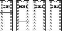
I2C and UNIO memories go in U4.
One-Wire devices in TO92 package use CONN6.
6 Or 8 pin 10Fxxx require an adapter not yet designed.
Some devices are limited to 3.3V, so a voltage regulator is included in the corresponding expansion boards.
The presence of the 3.3V adapter (which has RB1 and RB0 shorted) is checked by the software in order to avoid irreversible damage.
In some cases (e.g 16F1x o 18F), only the LF variant has this limitation, but this check is performed regardless (since the already long list of devices does not include sub-variants of every model).
Anyways, it is always possible to avoid this check via program options.
Target chips can also be programmed while still in the application circuit by routing ICSP signals to the application board. Low voltage devices require 3.3V ICSP signals, which are present on some of the low voltage expansion boards.
The ICSP-IN connector in the main board is used to program the main micro without extracting it, by means of another programmer.
The following images show how to insert various target devices in the expansion boards:
How to program the main micro the first time?
This is an interesting problem, a new device can't work as main programmer micro so it must be programmed in some way; a few options exist:- ask someone who owns a working programmer or a PICKIT.
- If you have a true RS232 port, build a serial programmer like JDM; use winpic or picprog software to do the job the first time.
- When using the 18F25K50, build a low voltage programmer out of an Arduino or ESP8266 or similar.
- Order a pre-programmed micro from MICROCHIP.
Make sure you program the device correctly. When using a 18F2550, do not enable the LVP bit (low voltage programming); this reserves RB5 for program mode entry and RB6-RB7 for communication, and the result is a non functioning programmer.
It would also be a good idea to buy a backup micro, in order to program it with updated firmware versions.
Map of resources and connectors:
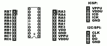
| Pin | Various functions | ICSP | I2C-EEPROM | SPI-EEPROM | SPI-ATMEL | uW-EEPROM | OneWire/UNIO |
| RB7 | PGM | ||||||
| RB6 | ICSP clock | ||||||
| RB5 | ICSP data | A2 | W (6) | ||||
| RB4 | A1 | HLD | S (1) | ||||
| RB3 | A0 | CS | Device clock | PRE (7) | |||
| RB2 | expansion | ||||||
| RB1 | Clock | Clock | SPI Clock | Clock | |||
| RB0 | Data | Data out (MISO) | Data out (MISO) | Data out | Data IO | ||
| RC7 | Data in (MOSI) | Data in (MOSI) | Data in | ||||
| RC6 | WP | WP | RESET | ||||
| RC5 | USB D+ | ||||||
| RC4 | USB D- | ||||||
| RC2 | DCDC PWM | ||||||
| RC1 | controls VDD | ||||||
| RC0 | controls VPP | ||||||
| RA5 | expansion | ||||||
| RA4 | expansion | ||||||
| RA3 | expansion | ||||||
| RA2 | LED 2 | ||||||
| RA1 | LED 1 | ||||||
| RA0 | ADC for regulator |
||||||
| RE3 | S1 switch |
Some photos of the various boards:
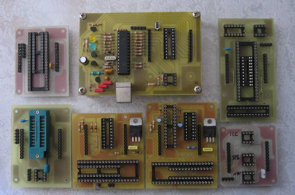
Expansion board connected to the main circuit:

OneWire device in TO92 package on an older version that did not have CONN6:
DCDC boost voltage regulator
In order to generate a voltage higher than 5V we need a boost switching converter.On the market there are thousands of single chip solutions, but I used instead the microcontroller itself and a few external components.
A fundamental requirement for this project is to be able to change the output voltage in real time.
The width of output pulses will vary to keep the output stable over all operating conditions.
In practice this is a digitally controlled regulator, as shown in the following diagram:
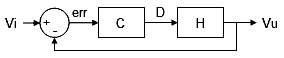
The ADC converter presently uses the 5V supply as a reference, so the output voltage will follow it; it is possible to connect an external reference to RA3 to improve the overall precision.
Switching frequency is 90 kHz, which is well over the cutoff frequency of the output LC filter (~2,3 kHz).
The performance is limited by losses due to the transistor, diode, inductor, but since the load is very low we can use low-cost (even recycled) components; to improve load capability switch to a better transistor, a Shottky diode, a higher rated inductor.
Anyways, in order to design a suitable regulator (block C above) it's necessary to work in s domain and model the converter itself; this has fortunately been done already, some info is available for example here.
With present component values the boost converter operates in dicontinuous mode; critical current is:
Icrit=Vu*T/(16*L)=86 mA
well over expected load, supposed to be 1 mA.
Other parameters:
Vi=5
Vu=12.5
D=(Vu-Vi)/Vo
L=100e-6
C=47e-6
I=1e-3
R=12/I
Rl=1.6 (inductor series resistance)
T=1/90e3
vu 1 vu M-1 Vu 2M -1
--- = Gdo ---------- where Gdo = 2 --- ------- , M = ---, wp = ----------
D 1 + s/wp D 2M -1 Vi (M-1) RC
--- = Gdo ---------- where Gdo = 2 --- ------- , M = ---, wp = ----------
D 1 + s/wp D 2M -1 Vi (M-1) RC
Transfer function results to be:
vu 127.58
-- = -------------
D 0.22031 s + 1
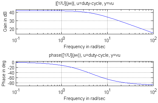
Which has the following Bode diagram:-- = -------------
D 0.22031 s + 1
It seems that the system, in closed loop, would be stable even by itself; however it would have a steady state error of 1/DCgain.
It's better to use a controller with a pole on the origin and a zero to stabilize everything, for example the following controller:
D 0.25 (s + 50)
C = --- = -------------
err s
C = --- = -------------
err s
Overall transfer function would be:
vu 144.77 s + 7238.4
-- = -----------------
vi s2 + 4.539 s
-- = -----------------
vi s2 + 4.539 s
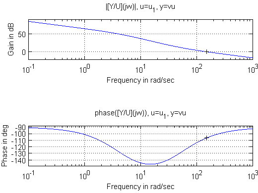
The system is stable, with a phase margin of ~75º.
Since we operate in the digital domain we must choose the sampling frequency.
It can't be too high because of execution speed; if too low it limits the regulator bandwidth; a period of 250 us was a good compromise.
The various transfer functions are converted to z domain using bilinear transformation:
vu 0.018199 z2+ 0.00022607 z - 0.017973
-- = ------------------------------------
vi z2 - 1.9989 z + 0.99887
The controller is:-- = ------------------------------------
vi z2 - 1.9989 z + 0.99887
D 0.25156*z - 0.24844 C1 - C2 z-1
C = --- = ------------------- = -----------
err z - 1 1 -z-1
Remember that z-1 represents a delay of one clock cycle.C = --- = ------------------- = -----------
err z - 1 1 -z-1
Next we must deal with quantization and calculation errors.
A/D converter is 10 bits wide, and is triggered by timer2; at the end of conversion an interrupt calls the regulation routine, which calculates the new duty cycle for the PWM peripheral, also 10 bits wide.
On the feedback path it's necessary to include a voltage divider in order to limit ADC input voltage to [0,5V]; R1 and R2 do this.
So the block diagram is modified as follows:
a=12/34
Vu=C'H(Vi-aVu)
Vu C'H
-- = ------
Vi 1+aC'H
To compare with the previous model we can multiply both terms by
a; simply remembering to change the set point we can decide that the
new input is Vi/a, and equate with the previous expression:-- = ------
Vi 1+aC'H
Vu aC'H CH
---- = ------ = ----
Vi/a 1+aC'H 1+CH
aC'=C---- = ------ = ----
Vi/a 1+aC'H 1+CH
aC1' - aC2' z-1 C1 - C2 z-1
aC'= --------------- = C = ------------
1 - z-1 1 - z-1
aC1'=C1aC'= --------------- = C = ------------
1 - z-1 1 - z-1
aC2'=C2
Since the hardware works with 10 bit digital data we can go from D/err to pwm/[err]:
[err]=err*1024/5
pwm=D*1024
D pwm/1024 pwm C1' - C2'z-1
C'= --- = ------------ = ------- = ------------
err [err]/1024*5 [err]*5 1 -z-1
pwm(1 - z-1)=[err](5*C1/a - 5*C2/a z-1)=[err](3.564 - 3.52 z-1)C'= --- = ------------ = ------- = ------------
err [err]/1024*5 [err]*5 1 -z-1
It's clear that integer multiplications can't be used with these coefficients; the easiest solution is to work with fractional values (i.e. divide output by 2N and multiply coefficients accordingly); considering that pwm output is 10 bits wide and left-aligned, we can easily work with values divided by 64.
pwm(1 - z-1)=[err](k1 - k2 z-1)/64
k1=5C1/a*64=228.12 ~ 228
k2=5C2/a*64=225.25 ~ 225
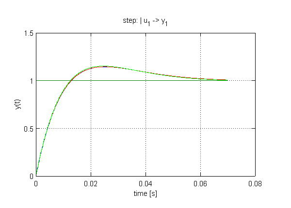
Following are step responses of continuous-time system (blue), discrete-time system (red), discrete-time system with approximate cefficients (green); As you can see they're almost coincident.
For all calculations I used Octave, an open source mathematical modeling tool; it can be used also under the famous windows (almost)operating system.
If someone is interested these are the modeling scripts I used.
The real code for the control function was written in assembly; this is necessary for performance reasons.
In fact our C compiler calls a library function to perform multiplications, so it has to save many variables on the stack causing a delay; in this case the resulting execution time had reached 50 us, which is a significant fraction of the sampling period.
Instead, by avoiding function calls and manually coding the 16x8 bit multiplication (see k1 & k2), the execution time is down to 12 us.
Some real waveforms:
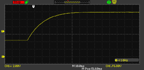
Power-up transient (12V)
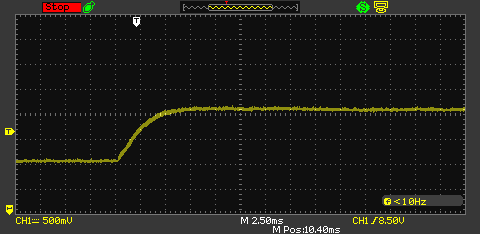
Step response to set point change (8V to 9V)
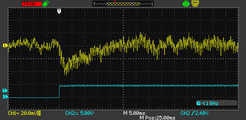
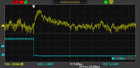
Step response to load change (0-1mA and 1mA-0)
How to contribute
The best way to contribute to this project is to build it, use it, and report bugs or suggestions.Also there are still many devices to test; check the list in supported devices.
Whoever has the know-how and patience can also expand support to other devices.
Or if you have a device that is not supported you can send it to me so that I can work on it.
If you find this project useful write me a couple of lines:
 ,
and if you modified it show me your work.
,
and if you modified it show me your work.On SourceForge you can find some forums where you can discuss about this project; you could also recommend it or write a (hopefully positive) review.
Downloads
Schematic diagram and pcb: Pdf, complete archiveFirmware: complete MPLAB project or firmware compiled for 18F2550(.hex) or for 18F25K50(.hex)
opgui (GTK GUI for Linux & Windows): sources or application
OP (command-line for Linux & Windows)
Opgui user's guide
Octave scripts
History
| the future | increase support for PIC and ATMEL micros; add JTAG; expand ICD support |
| December 2023 | opgui v0.12.2: fixed config write on 16F18456; support all-in-one board |
| February 2023 | opgui v0.12.1: fixed crash when selecting "*" filter |
| October 2022 | firmware v0.12.0: adapted to 18F25K50; opgui v0.12.0: port to GTK3; device selected via tree; send manual commands; op/opgui: added 16F15213-14-23-24-25-43-44-45-54-55-56-74-75-76, 16F18013-14-15-23-24-25-26-44-45-46-54-55-56-74-75-76, 16F18114-15-24-25-26-44-45-46-54-55-56-74-75-76, 16F17114-15-24-25-26-44-45-46-54-55-56-74-75-76, 18F04-05-06-14-15-16Q40-41, 18F24-25-26-44-45-46-54-55-56Q71, 18F26-27-46-47-56-57Q83-84; fixed write on 254005 |
| December 2021 | software v0.11.5: fixed config word write on some 33FJXX devices |
| July 2021 | software v0.11.4: minor corrections |
| April 2021 | software v0.11.3: fixed EEPROM write on 16F184xx/188xx/191xx |
| December 2020 | circuits v2.1: added pull-down on AVR expansion board |
| October 2020 | firmware v0.11.2: extended ICSP8_READ payload to 16 bits (for PIC18) software v0.11.2: fixed 16F18xxx write with empty space at address 0; added 18F25-26-27-45-46-47-55-56-57Q43, 18F25-26-27-45-46-47-55-56-57K42, 18F25-26K83 [linux] changed HW access path to /dev/hidraw circuits v2.0: ported to kicad, offset expansion connectors |
| February 2020 | software v0.11.1: fixed save file for 12F1XXX; fixed timeout writing config for 16F18XXX; avoid reading DIA-DCI on 16F188XX; fixed EE verification of 0x22 on 18FXXX |
| January 2019 | firmware v0.11.0: added instructions ICSP8_SHORT,ICSP8_READ,ICSP8_LOAD; software v0.11.0: added 16F15313-23-24-25-44-45-54-55-56-75-76-85-86, 16F18424-25-26-44-45-46-54-55-56, 16F18854-55-56-57-75-76-77, 16F19155-56-75-76-85-86-95-96-97 |
| December 2018 | software v0.10.1: added 16F1764-65-68-69-73-76-77-78-79; removed MSVC6 function definitions |
| June 2016 | firmware v0.10.0: added instructions LOAD_PC, LOAD_DATA_INC, READ_DATA_INC, JTAG_SET_MODE, JTAG_SEND_CMD, JTAG_XFER_DATA, JTAG_XFER_F_DATA; new USB VID&PID (0x1209,0x5432); changed some CK timing; reduced CLOCK_GEN startup time; software v0.10.0: added 16F18313-23-24-25-26-44-45-46; improved USB communication |
| November 2014 | software v0.9.1: various user interface improvements;
fixed verification of ATTiny11-12; fixed 24FJ128GA3xx-GB2xx-GCxx-DAxx;
added: config force for PIC18, IO lines hardware test,
AVR auto speed communication, AVR write fuse @ 3kHz;
faster write verification for SPI FLASH memories; added 10F320-22,12F529T39A,12F752,12F1612-13-14-15-18-19, 16F1512-13,16F1574-75-78-79,16F1703-04-05-07-08-09-13-16-17-18-19, 16F1788-89,16F570,16LF1554-59, 18F24K50-25K50-26K50-45K50-46K50, 18F25K80-26K80-45K80-46K80-65K80-66K80, 18F63J11-90,18F64J11-90,18F65J10-11-15-50-90, 18F66J10-11-15-16-50-55-90-93,18F67J10-11-50-90-93, 18F83J11-90,18F84J11-90,18F85J10-11-15-50-90, 18F86J10-11-15-16-50-55-90-93,18F87J10-11-50-72-90-93, 25X128,25Q40 |
| March 2014 | firmware v0.9.0: support for ATMEL HV serial programming; new command for PIC24/33; improved DCDC regulator; software v0.9.0: Write16F72x requires only config-word 1; added HV serial programming for ATtiny11-12-13-24-25-44-45-84-85; added 24FJ64GA3xx-GCxx,24FJ128GA3xx-GB2xx-GCxx-DAxx,24FJ256DAxx,24EPx,33EPx; added 95xx SPI EEPROM,25X05 FLASH; added 12F1571-72,16F527,16F753,16F1454-55-59; some code rework & minor improvements; |
| June 2013 | software v0.8.1: various user interface improvements; fixed EEPROM write when code protection is active (16F83-84,12F629, 12F675,16F627-28,16F630,16F676,16F870-1-2,16F873-74,16F876-77); fixed read of files > 1MB; modified prog mode entry for AVR; fixed write of 93Sx6 with protection; |
| July 2012 | firmware v0.8.0: support for One-Wire and UNIO; software v0.8.0: added DS2430,DS2431,DS2433,DS28EC20,DS1820; 11010-20-40-80-160; 251005,252005,254005,258005,251605,25X10,25X20,25X40,25X80, 25X16,25X32,25X64; 16F1782-3-4-6-7,12C508-9; corrected write for 24x1024/5 and 251024; |
| January 2012 | software v0.7.10: added 12F617,12F1501,16F1503-7-8-9,16F720-21,16F72,16F707, 18F13K22,18F14K22,18F23K22,18F43K22,18F24K22,18F44K22,18F25K22, 18F45K22,18F26K22,18F46K22,18F8520,18F66J60,18F66J65,18F67J60, 18F86J60,18F86J65,18F87J60,18F96J60,18F96J65,18F97J60, fixed read/write binary files, various corrections, added support for in-circuit debugging in OPGUI |
| June 2011 | software v0.7.9: added ATtiny11-12-24-26-261-44-48-461-4313-84-88-861,
ATmega48-88-164A-168-324A-328-644A-1284, 16LF1902-3-4-6-7,
various minor modifications and fixes; new graphical interface based on GTK for Linux and Windows |
| April 2011 | software v0.7.8: updated algorithms for 16F87xA and 16F62xA, 16F1822 becomes 12F1822, added 30F1010, 30F2020, 30F2023, 16F1847, 12F1840 16F1516, 16F1517, 16F1518, 16F1519, 16F1526, 16F1527; greater modularity for source code, corrcted some bugs |
| August 2010 | software v0.7.7: added 16F72x, some minor fixes; circuits v1.7.1: reduced value of R173 on the PIC16/18 LV expansion board |
| July 2010 | firmware v0.7.6: modified TX16 and RX16 with variable period for communication with ICD; software v0.7.6: byte by byte read with 93xx6 for better compatibility; first release of pdb debugger (v0.1); |
| June 2010 | software v0.7.5: corrected write bug for 18Fx config, added "goto ICD" write for 16Fx, various minor fixes |
| May 2010 | software v0.7.4: added PIC18FxJx, PIC18FxKx, PIC24H, dsPIC30-33, ATtiny2313, 241024; bugfix; circuits v1.7: modified PIC24-30-33 expansion board, PIC30 now at 5V |
| April 2010 | software v0.7.3: added PIC16F1xxx; OP works in windows; code rework and bugfix; circuits v1.6: expansion board for 3.3V PIC16-18 |
| March 2010 | software v0.7.2: added some MicroWire eeproms; bugfix |
| February 2010 | software v0.7.1: added some PIC18 and Atmel devices; bugfix |
| January 2010 | version 0.7.0: added PIC24 and SPI EEPROMs; circuits v1.5: expansion board for 3.3V PIC24-30-33 |
| October 2009 | software v0.6.2: bugfix |
| September 2009 | version 0.6.1: solved some SPI bugs, added some Atmel devices and 93Cx6C |
| June 2009 | version 0.6: fully GPL2 USB firmware, added 93Sx6 MicroWire EEPROMs |
| April 2009 | schematic diagram and pcb v1.4: changed Atmel adapter |
| March 2009 | software v0.5.2 and v0.5.3: added some PIC an Atmel devices, removed some bugs |
| January 2009 | software v0.5.1: added some PIC devices, removed some bugs |
| November 2008 | version 0.5: I2C & SPI bus, added some ATMEL devices |
| August 2008 | version 0.4: added support for I2C EEPROMs |
| July 2008 | documentation and website, released version 0.3 |
| 2008 | first prototypes and software |
| 2007 | experiments with USB PIC and varionus firmwares; voltage regulator |
| a long time ago | need for a reliable and free USB programmer |
Links
Open Programmer on SourceForgeQuick guide to a HID firmware
pdb, a simple ICD debugger for PIC16
openprog_tools, a fork of op/opgui
MSYS2, official toolchain for windows
GTK3 runtime, graphical libraries for windows
KiCad
Microchip (and Atmel)
USB 2.0 standard
HID page on USB.org
USB & PIC
hiddev documentation
ICprog
Octave
gEDA project
GNU/GPL
Piklab IDE for PIC microcontrollers
USBPicprog, another open source programmer
Cygwin, a linux environment inside windows
Contacts
For informations or comments:Alberto Maccioni
You can also post your questions on the forum on sourceforge.